Product Portfolio
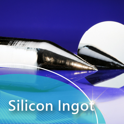
Silicon Ingot
Ingot is grown for customer specific orientation; by using different dopants the type and resistivity are determined. We provide low impurity and high quality ingots for all kinds of products.
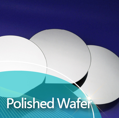
Polished Wafer
Polished wafers are silicon wafers that are mirror-polished on one or both sides.
Polished wafers, with excellent characteristics such as high flatness, high cleanliness,
and proper gettering, have earned a reputation as high quality, high precision products
that meet the needs of advanced memory devices, etc.
They are used for electric power control devices and integrated circuit applications by
our customers.
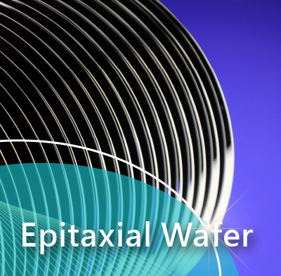
Epitaxial Wafer
Epitaxial wafers are the traditional wafers to achieve surface integrity by putting various
thickness epitaxial silicon layers.
Thin Epi wafers are commonly used for leading edge MOS devices.
Thick Epi or Multi-layered epitaxial wafers are used for the devices mainly to control
electric power, and they are contributing to improving the efficiency of energy consumption.
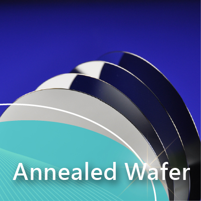
Annealed Wafer
- 1. Hi-WAFER Hi-WAFER(Hydrogen Annealed Wafer) is heat treated in hydrogen ambient, and realized high BMD density which provides gettering ability as well as COP-free zone in the wafers surface region. These properties contributes to have excellent gate oxide quality.
-
2. Hyper Hi-WAFER
AT-WAFER is also an annealed wafer, but heat treated in Argon gas ambient to prevent
outdiffusion of dopant from wafer surface and to have flat resistivity profile in depth.
AT-WAFER serves the same quality as Hyper Hi-WAFER® in other aspects.
These wafers were developed for use in miniaturized devices and feature a flat boron profile around the surface.
Wafers for advanced miniaturized products contribute to the miniaturization of LSI devices, and device process miniaturization contributes to energy saving in the form of reduced operating voltage. -
3. AT-WAFER
Hyper Hi-WAFER® (hydrogen annealed wafers) were developed for cutting-edge devices.
The improved crystalline technology, optimized hydrogen treatment, and improved processing techniques have resulted in improved internal gettering and flatness properties compared to conventional Hi-WAFER®, as well as reduced LSTD density.
Electrical characteristics such as junction leakage characteristics have been further improved compared to conventional silicon wafers as well as Hi-WAFER®.
They also have excellent flatness characteristics to allow miniaturization.
Wafers for advanced miniaturized products contribute to the miniaturization of LSI devices, and device process miniaturization contributes to energy saving in the form of lower operating voltage.
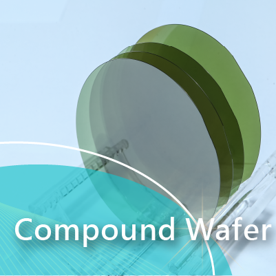
Compound Wafer
Recently power device and communication technology grow fast, the requirement for
substrate is getting higher.
Traditional Si substrate couldn’t fulfill the requirement of latest technology, GaN
and SiC material become one of the best solution.
GaN and SiC material both possess wide band gap property, it is good for high breakdown
and high temperature application, very suitable for high power product.
GaN material also possess high electron mobility property, combine with semi-insulating
SiC substrate, it shows great advantage on high frequency communication application.
GaN and SiC are next generation key semiconductor material.
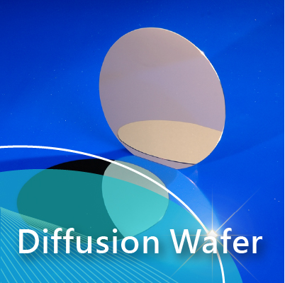
Diffusion Wafer
Diffused wafer is employed in electric power control devices frequently and contribute to
improving the efficiency of energy consumption.
Our Diffused Wafers which ensured accurate diffusion concentration, diffusion depth and
undiffused width through precisely controlled process are easy for users to control in
the manufacturing process and offer superior products with favorable conditions for
device design has been well received as.
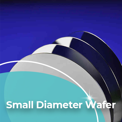
Small Diameter Wafer
For small-diameter wafers conventionally, chemical etched backside has been the global
standard for semiconductor use.
In recent years, we have received requests from customers who want thin wafers and also
need the equivalent polishing quality on the backside as the top surface for various
sensing devices like detectors, or customers who want superior flatness for substrate
materials for MEMS, SAW filter devices.
To respond such VOCs, we applied the high-precision processing technology that we have
cultivated through production of the diffused wafers and the thick SOI wafers, the
double-side-polished wafers with <=150mm Diameter and superior flatness have been
commercialized.
For the crystals, the Czochralski method (CZ, MCZ) which is the most common for silicon
single crystals, and also the float zone method (FZ) which can be achieved extremely
low interstitial oxygen concentration and ultra high resistivity are available to be
provided
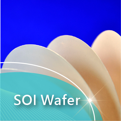
SOI Wafer
SOI enables increased chip functionality without the cost of major Fab process equipment
changes.
Faster circuit operation and lower operating voltages have produced a powerful surge in
the performance of high-speed network servers and new designs for hand-held computing
and communication devices with longer battery life. Advanced circuits, using multiple
layers of SOI-type device silicon, can lead the way to a coupling of electrical and
optical signal processing into a single chip resulting in a dramatic broadening of
communication bandwidth and new applications such as global-ranging, direct-link
entertainment and communication to hand-held devices.
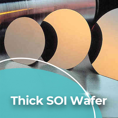
Thick SOI Wafer
Ordinary bonded Thick SOI wafers took the "Terrace structure" in order to remove un-bonded
area around periphery of wafer. This terrace sometimes may cover up to approximately 10%
area of the wafer surface.
We have been able to provide Thick SOI wafers without the "Terrace" so called "Terrace
Free structure" by controlling diameter of both substrates.
This unique structure can help customers handle the Thick SOI wafers on the same
processing as regular wafers, and consequently give larger device manufacturing area
for in a wafer.
Thick SOI wafers are widely used in power devices and MEMS to achieve high breakdown
voltage, low energy consumption and high performance of MEMS. This is possible due to
their SOI structure.
We use a bonding method in the manufacture of thick SOI wafers and exercise more precise
control over the thickness of the SOI layer and the BOX layer.
The demand for SOI wafers in leading-edge devices such as intelligent power modulus,
which require high breakdown voltage and low energy consumption, is also increasing.
More over MEMS made of SOI brings complex 3-D structure such as accelerometer and
pressure sensor.